


Όπως είναι γνωστό, ο σχεδιασμός big.LITTLE της ARM που συναντούμε στην πλειονότητα των SoCs (System-on-Chips) για φορητές συσκευές δεν αποτέλεσε πηγή έμπνευσης μόνο για την Intel αλλά υπάρχει στα πλάνα της AMD εδώ και καιρό.
Πρόσφατα, η γνωστή εταιρεία σχεδίασης επεξεργαστών κατοχύρωσε δίπλωμα ευρεσιτεχνίας για την δική της υβριδική τοπολογία πυρήνων επεξεργαστή που είναι εμπνευσμένη από την «αρχιτεκτονική» big.LITTLE της ARM -όπως άλλωστε αποτέλεσε πηγή έμπνευσης και για τους υβριδικούς επεξεργαστές της Intel που θα δούμε τα επόμενα χρόνια. Σύμφωνα με την καινοτομία big.LITTLE ένας επεξεργαστής μπορεί να διαθέτει δύο διαφορετικούς τύπους πυρήνων με πολύ διαφορετικές σχέσεις performance/ watt, με τον έναν τύπο να αναλαμβάνει ροές εργασίας υψηλής απόδοσης και τον άλλον να αναλαμβάνει τις πιο «ελαφριές» εργασίες. Κάτι τέτοιο μοιάζει απλό θεωρητικά, ωστόσο στην πράξη είναι ένα αρκετά δύσκολο εγχείρημα, ειδικά στην περίπτωση που οι διαφορετικοί πυρήνες (ετερογενής σχεδίαση) κάνουν χρήση άλλου αρχιτεκτονικού σχεδίου ή ενσωματώνουν διαφορετικά σετ εντολών.
Η AMD, στην αίτηση κατοχύρωσης διπλώματος ευρεσιτεχνίας, περιγράφει μία μέθοδο για την άμεση εναλλαγή της επεξεργασίας των ροών εργασίας μεταξύ των δύο διαφορετικών τύπων πυρήνων. Σε αντίθεση με τα ομογενή αρχιτεκτονικά σχέδια επεξεργαστών όπου μία ροή εργασίας που έχει αναλάβει ένας πυρήνας συνεχίζεται διαμέσου της L3 cache για παράδειγμα, στη περίπτωση της πατέντας της AMD, οι δύο πυρήνες αλληλοεπιδρούν μέσω ενός προηγμένου υπερσυνδέσμου που χρησιμοποιείται και για την επικοινωνία διάφορων άλλων στοιχείων του επεξεργαστή (π.χ. I/O, ελεγκτή μνήμης, iGPU). Σύμφωνα με την AMD, η εναλλαγή μεταξύ των πυρήνων εξαρτάται από μία σειρά από παράγοντες όπως από την ανάγκη χρήσης σετ εντολών που βρίσκονται μόνο στους υψηλής απόδοσης πυρήνες, το CPU core utilization, το memory utilization, την ανάγκη για εξοικονόμηση ενέργειας (που είναι και βασικός στόχος μίας τοπολογίας big.LITTLE) κ.ά.
Σύμφωνα με φήμες, οι πρώτοι επεξεργαστές της AMD που θα κάνουν χρήση ενός σχεδιασμού τύπου big.LITTLE θα είναι οι αρχιτεκτονικής Zen 5, «Strix Point» που δεν αναμένεται να λανσαριστούν πριν από το 2024 και θα ονομάζονται Ryzen 8000 series κατά πάσα πιθανότητα. insomniagr
NEW AMD X86 LITTEL TECHNOLOGY

It’s become clear that hybrid cores — big.Little in ARM’s parlance — are going to be a feature of mainstream x86 CPUs as well. Intel’s Lakefield combines one Ice Lake “big core” with four Tremont “little” cores. Its upcoming Alder Lake platform will scale the solution up, with (rumored) up to eight low-power cores (Gracemont) and eight high-performance cores (Golden Cove).
More details on AMD's version of big.LITTLEhttps://t.co/OwsdshPV7G pic.twitter.com/T55kM5Yg1w
— Kepler (@Kepler_L2) June 12, 2021
A few signs have indicated AMD has its own plans to get into this game, and a new patent filing backs up that idea. AMD has applied for a patent describing methods by which one type of CPU would move work over to another type of CPU:

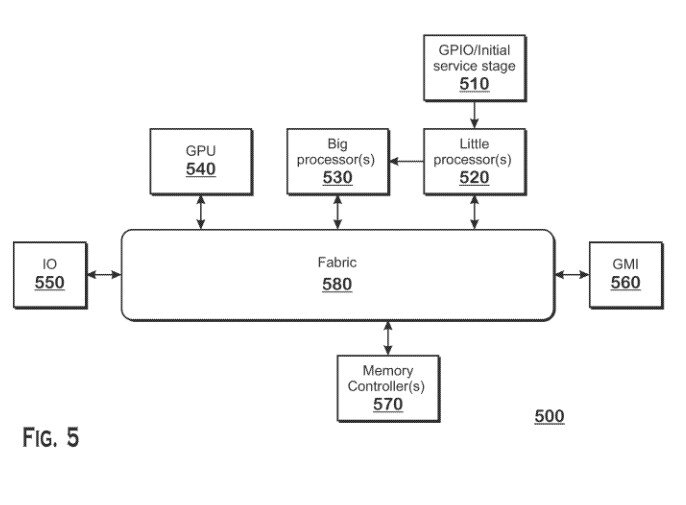
Figure 5 from AMD’s patent application.
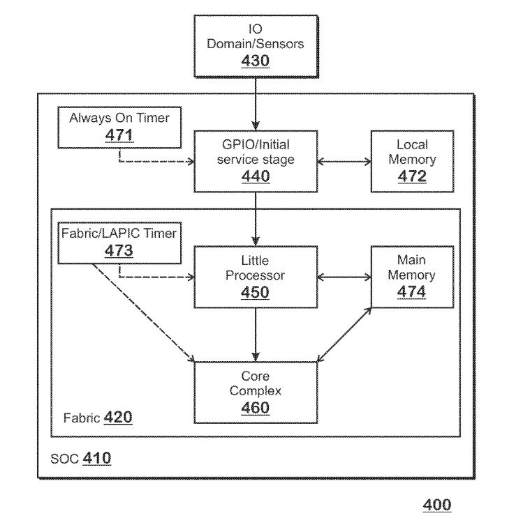
According to the patent, CPUs would rely on core utilization metrics to determine when it was appropriate to move a workload from one type of CPU to the other. Proposed metrics include the amount of time the CPU has been working at maximum speed, the amount of time the CPU has been using maximum memory, average utilization over a period of time, and a more general category in which a workload is moved from one CPU to the other based on unspecified metrics related to the execution of the task.
When the CPU determines that a workload should move from CPU A to CPU B, the core currently performing the work (CPU A, in this case), is put into an idle or stalled state. The architecture state of CPU A is saved to memory and loaded by CPU B, which continues the process. AMD’s patent describes these shifts as bi-directional — the small core can shift work to the large, or vice-versa.
big.Little Won This Fight
Ten years ago, I asked Intel’s smartphone SoC designers why they were relying on DVFS — Dynamic Voltage and Frequency Scaling — to keep Atom’s power consumption competitive rather than big.Little. According to Intel’s architects, DVFS was competitive with what big.Little could deliver when one considered the silicon die space requirements and the overall power savings.

That may have been true at the time — Medfield was generally competitive with the midrange Cortex-A9 devices it was intended to compete against — but it doesn’t seem to be true today. At the time, Medfield was built on the 32nm process node, while the Cortex-A9 was generally built on 40nm or 28nm. Even if we count conservatively, TSMC and Intel have been through multiple full node shrinks. Intel’s 10nm technology is considered equivalent to TSMC’s 7nm node. The die size penalty for using a hybrid x86 core design is much smaller than it used to be.


0 Post a Comment:
إرسال تعليق